Why Have ALUs on a Memory Die?
Wednesday December 16, 2020By Mark Baumann
Director, Product Definition & Applications MoSys, Inc.
If we review what issue everyone faces with memory, it tends to revolve around the challenge of getting data on and off the die. With memory, it is a very common desire to access a piece of data (which requires a Read operation) followed by some manipulation of the data that was just read which can entail an add, compare, logical operation like an OR, AND etc. This will all result in an action as to what to do next with the data and the final operation on the data is to store the result back into the memory (which entails a Write operation).
If we look at what took place, it is what is commonly known as an RMW or Read-Modify-Write operation. This is a very common function in systems to perform functions like statistics or to decide if a piece of data is greater than or less than and many other operations are a result of some basic ALU operations. In order to accomplish these functions, the main “hit” in accomplishing this is the time it takes to go retrieve the piece of data from memory and the resulting write operation when the ALU operation is complete.
The bottom line is that it takes time and effort to issue a read, which has the issuing entity drive a command and address off its die and onto a bus and then it received by the memory device, performs the read operation, then drives the bus again and is received by the issuer.. This all takes time and power to accomplish. In an effort to minimize both, it seemed to make sense to move the compute resource closer to the storage. In doing so, the time and power associated with two-thirds of the operation is saved. All that is needed is to issue a single command with a piece of data, and the operation of the ALU can be performed on the memory die rather than transfer data and commands back-and-forth between two devices on a PCB.
This involves the memory silicon having a relatively simple block of logic resident on it’s silicon and the savings can be significant and measurable in both performance and power.
In the following figure, the internal data paths are depicted that are associated with the addition of an ALU on the silicon. As can be seen, it is not quite that extensive. However, like most items, there are always some additional overhead to be considered. In this case it is ECC (Error Check and Correct). As a precaution, the die will also maintain ECC on data that is associated with an ALU operation. This is a precaution to ensure that any piece of data that will have an operation performed on it is, first checked for accuracy. This requires that on the memory die an ECC operation is first performed on the data, which will ensure that the data integrity is maintained. When the data is read, it will initially be checked for correctness by performing an ECC operation. If the data is verified as valid, the modification operation can be performed. If, however, a bit error is identified the ECC logic will correct the error before data modification, then the data can be safely modified. This is a precautionary step to maintain data integrity.
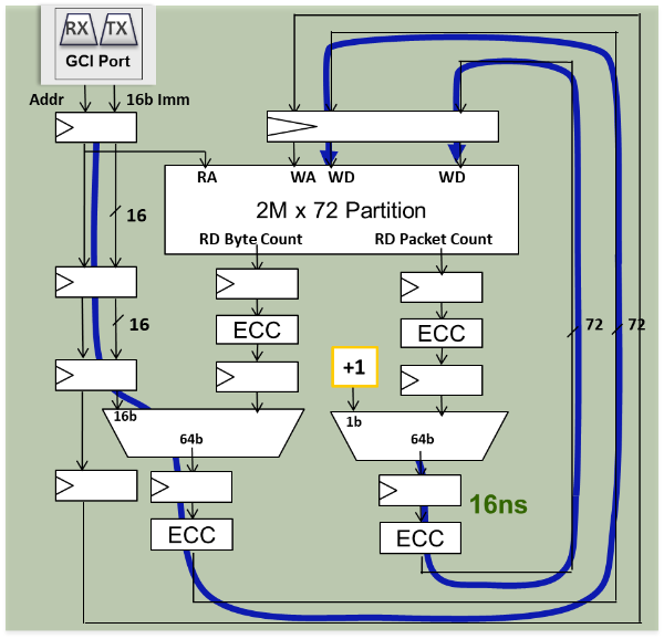
In the following figure, it can be seen that the ALU logic itself is a block that is placed at strategic locations within the silicon to allow for multiple operations to happen concurrently. It is a small enough block of logic that it is possible to have multiple instantiations and not impact either die size or power.
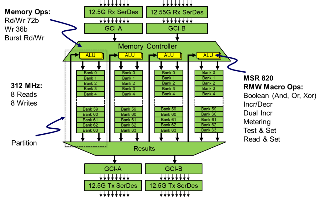
The tradeoff that MoSys has made was that this small amount of logic was a good addition for the potential system gains. We have been able to support maintaining Byte and Packet counts on up to 32 – 100GE-ports in a single device.
What we are wanting to illustrate, is that for a small investment in space, there can be a measurable benefit to a systems functionality and performance. When adding a simple ALU to the silicon, it allows a user to offer a feature like maintaining statistics that otherwise would eat up valuable space in the controller ASIC or FPGA. It also saves power by minimizing the amount of bus transitions that are required to perform a simple, but powerful ALU operation.
It is believed that this “trend” of placing intelligence closer to storage elements will continue. In fact, MoSys has taken the concept even a step further with the Programmable HyperSpeed Engine (PHE) which has placed 32 multi-threaded RISC cores on a 1Gb memory die. Stay tuned for more details on this in a future blog!
Additional Resources:
If you are looking for more technical information or need to discuss your technical challenges with an expert, we are happy to help. Email us and we will arrange to have one of our technical specialists speak with you. You can also sign up for updates. Finally, please follow us on social media so we can keep in touch.