Not All Memory Chips Are Created Equal
Thursday September 2, 2021By Mark Baumann
Director, Product Definition & Applications
MoSys, Inc.

What do you want from a memory chip? The most likely and common answer to that question is storage. When we look at what memory is used for, it is basically storage. And all the different variations of memory, ROM, DRAM, RLDRAM, SRAM etc., up to the memory of the most recently acclaimed HBM. All these devices are designed with storage as the first purpose to provide to a user.
As most of us know, every type of device has it benefits and drawbacks. ROM (Read Only Memory) is great for storage of non-volatile and static data; most other types of storage is made to be changeable and allow for both Reading of Data and writing. This would be Flash, DRAM and SRAM based devices. Again, each of these devices are designed to fit in a certain area of need.
Flash is very dense and can maintain data even if power to the system is lost, which is why this is the most common technology used in current SSD (Solid State Drive) devices. The drawback is the time it takes to write data into this NAND-type memory. But this is a tradeoff for the non-volatility of the technology.
DRAM or Dynamic Random-Access Memory is again a technology that is designed for density of storage, allowance for reading and writing. This is the most common of Random-Access type storage devices. But as with anything, there is a drawback and that is the Random Access in the device can have some severe limitations with the concerns of tFAW and Refresh. These result in a potentially non-deterministic access latency.
SRAM or Static Random-Access Memory is again addressing an area of need for fast Write and Read capability and a very deterministic access latency. This technology was designed to provide speed of access and deterministic access time. The drawback of this technology is that the density is much lower than other technologies and the power is higher due to the desire to run at higher frequency.
So, this has been a roundabout way of stating that there has yet to be designed a memory that addresses the needs of all. The latest memory trend is a spin on DRAM with the acronym of HBM (High Bandwidth Memory). This is a wonder of technology in that it allows for VERY high density by stacking DRAM Die on top of each other and using Through Silicon Vias (TSV) to connect the multiple die together. This allows for a new Z or height dimensional aspect to the density of memory. The issue that comes along with HBM, is that the base technology is still DRAM and the stack of die still suffer with the base limitations of DRAM regarding random access and the need for refresh. On the other hand, the shear bandwidth that is possible with HBM stacks is impressive. This potential bandwidth is severely impacted when there is a need for random access to the stored data.
In any instance, the desired or chosen memory performs it’s job of data storage; with the associated tradeoffs of the associated underlying technology. The next level of consideration is what needs to be done with the data that was stored. In the case of FLASH memory, it needs to be reliably stored, even during power loss, and be readable frequently but written very infrequently. In the case of DRAM and SRAM, the need tends to center around the necessity to change the data that is stored and therefore there is a requirement to both read and write the data in the memory. In any case, the need to READ the data is always present. The action of reading is done for a purpose, in most cases the data being read is needed so that the information being read will allow for a calculation or decision to be made for a next action to be taken.
Examining this aspect, it is clear that this will take time: the act of reading where a host device needs to issue a read, sending the command across a bus to the memory, the memory then receives the command and executes the memory access and the data is then sent back across the bus to the host device that now receives it. It then performs as an action on the data and may even potentially need to write it back to the memory device for later access. All this, as I said, takes time and impacts the throughput that can be achieved for the system.
When MoSys looked at this impact on system throughput, it seemed clear that some improvements on system throughput can be achieved by simply moving the ability to perform an action on the data, actually on the memory die and how this could potentially save significant bus bandwidth and improve system throughput. To this end, MoSys has developed two families of memory devices that have In-Memory Functions (IMF). The first device is a memory device with ALU capability on-die (see the figure below).
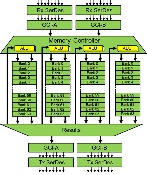
By making the ALUs available, which are capable of performing both logical and arithmetic operations, on the die with the memory, the host device only need send a command across to execute operations like counter updates, statistics or even metering calculations. This frees up the host and the bus to perform other operations.
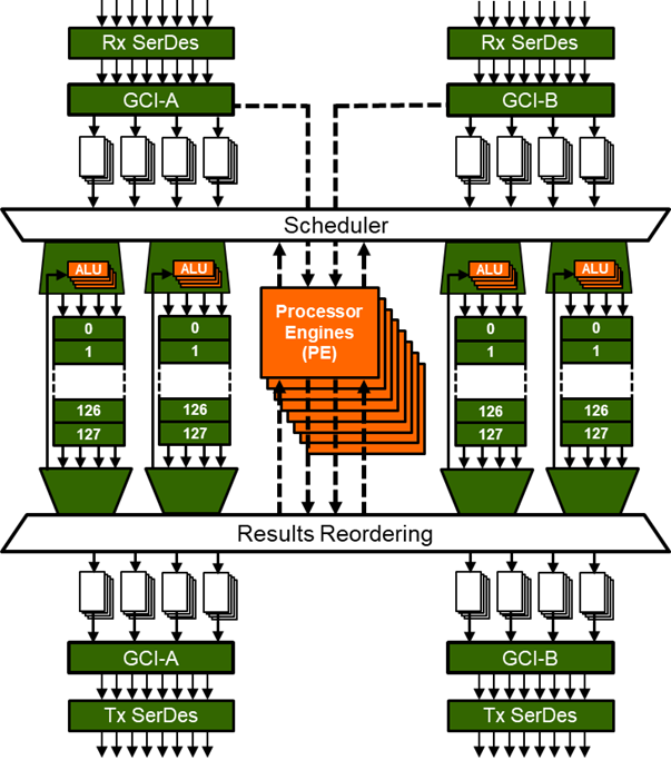
In a second device that MoSys offers, the level of IMF is greatly increased. In this device are 32 multi-threaded RISC cores that can de-programmed to implement a user-defined function or algorithm — with full access to the on die stored data. This will potentially free up significant host overhead and act as a supplemental offload to system resources. This provides the ability for the used to implement a system boosting algorithm or support function that previously was unattainable with a pure memory device (see the diagram below).
With the ability that these two MoSys families of devices provide, it opens a new way to look at storage. Not all memory chips are created equal. Although at the base level they all provide storage, this new MoSys family of In-Memory-Function devices provide a more efficient way to utilize this storage and open up new features and functions for a system. By moving the compute logic to the memory, it not only adds efficiency but allows the design to distribute the compute function to where it provides the greatest benefits.
If you wish to explore how these devices can benefit your system or to just learn more about the features and functions of these devices, please contact MoSys Sales or Applications.
Additional Resources:
If you are looking for more technical information or need to discuss your technical challenges with an expert, we are happy to help. Email us and we will arrange to have one of our technical specialists speak with you. You can also sign up for updates. Finally, please follow us on social media so we can keep in touch.