How Board Design Can Expedite Your Next Design Project
Thursday June 10, 2021Part 2 of 2
By Mark Baumann
Director, Product Definition & Applications
MoSys, Inc.
MoSys recently hosted a webinar with our distribution partner Arrow. The focus was board design guidelines which, on the surface, appears to be a rather mundane topic. The reality is, however, that a properly designed board can save time and money while accelerating time to market. As a quick reminder, the reason MoSys is interested in this topic is due to the fact that our product offerings are based on the use of high-speed SerDes as the I/O structures:
In Part 2 of this blog we will cover trace matching, reverse polarity, layout of AC coupling caps, power integrity, and a summary of first order considerations for channel design.
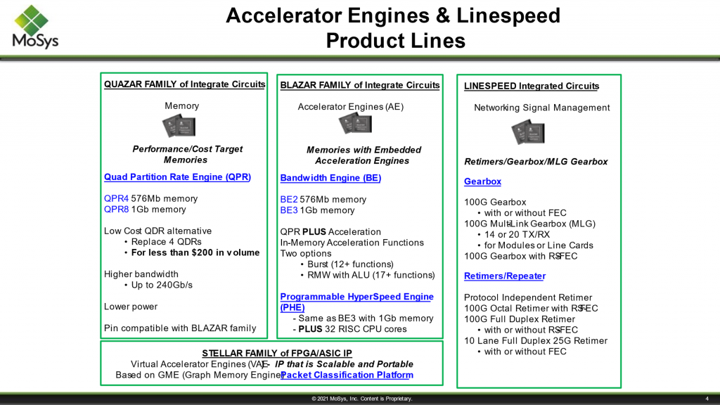
Trace Matching
The figure below has a length mismatch due to the ballout at the device. The wiggle pattern is used to increase the length of the shortest trace, to balance it with the longer trace. The wiggle in the trace should stay as close to the source of the original mismatch as possible and in some cases this may be hard to accommodate for example the trace to the right of #1 has the length equalization mid-way, but this is still as close to the origin of the mismatch as possible.
Signal Polarity
Another option that is available in most SerDes links is to not be concerned with matching the polarity of the differential pair. In most cases it can be reversed for both transmitter and receiver; the TXP from the host can go to RXN. In addition, TXN can go to RXP, as the design can internally correct for the polarity. This feature gives freedom to a layout engineer to reduce, length, simplify routing and possibly more accurately match trace length.
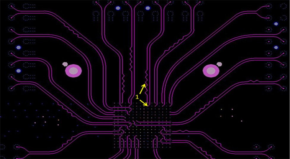
AC Coupling Caps
It should be noted that AC coupling capacitors are sometimes required for high-speed signals. In this case, choose an AC coupling capacitor that has a size that is about the same width as the signal traces and ensure that the characteristic impedance of the components match as closely to the signal impedance. Illustrated below where 0201 size 0.1uF capacitors are slightly wider than the traces and would cause a capacitive discontinuity. To compensate for this, the ground plane underneath the component is partially cut out. This this is not ideal, as it makes the ground return not uniform.
Power Supply
To reduce supply ripple voltage, it is generally recommended to use power planes in the PCB with alternating VDD/GND layers. Place capacitors as close to the device as possible to minimize inductance in the PCB traces that connect to the capacitor. Then, treat the supply, the GND as well as parallel path of decoupling capacitors as a continuous plane. Place the VDD and VSS vias adjacent as pairs to minimize inductance and obtain di/dt information for each supply
It is generally recommended to use a range of decoupling capacitors to reduce the ESR over a wide frequency range – e.g. capacitors at 100, 10, 1, and 0.1uF.
Be sure and review:
- Bulk Decaps – Check if quantity and values are sufficient for filtering
- Decap-Mid and High freq – Check if quantity and values are sufficient for filtering
- Tantalum Caps polarity visible and properly connected
- Check if Caps have sufficient Voltage rating: generally recommend >2.5X rating
- Check if Ferrite bead used when a power supply is shared between analog and digital domain.
- Check if Ferrite bead DC resistance is low such that the power supply voltage level is within tolerance.
- Check if Ferrite bead chosen have sufficient current rating
Make sure that sense line(s) are connected very close to the load and with respect to signal attenuation, routability must be properly balanced with trace width selection for better performance.
Crosstalk
To address crosstalk, crosstalk control usually involves reducing signal edge rates and maintaining enough trace-to-trace separation to reduce the mutual capacitive and mutual inductive coupling energy. Note that reducing the signal edge rate is usually not an option. Crosstalk control for high-speed transceiver designs is mainly determined by PCB layout spacing constraints to keep the transceiver traces far enough apart to minimize the coupling effect. Microstrip routing requires a larger separation to properly manage the crosstalk. Stripline routing requires only smaller separation to achieve reduced crosstalk.
1st Order Layout Considerations
For high-speed transceiver signals, use trace widths of 6mils or more to minimize conductor loss. Be sure and limit use of 4-mil trace widths to the BGA breakout area and keep their trace length as short as possible and note that loosely coupled traces are easier to route and maintain impedance control. Tightly coupled traces saves routing space but can be difficult to control impedance.
Use strip-line routing, wherever possible to avoid FEXT concerns.
C-via optimization include reducing the via capture pad size, eliminating all non-functional pads (NFP), and increasing the via anti-pad size to 40 or 50 mils.
Lvia optimization include eliminating and / or reducing via stubs, minimizing via barrel length by routing near the strip-line traces near the top surface layer and applying back-drilling. Additionally, add ground return vias as close as possible to each signal via in order to further improve the insertion and return losses of the via.
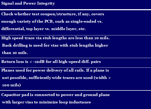
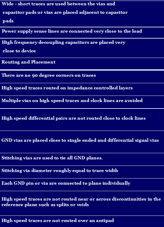
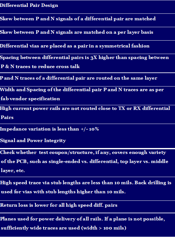
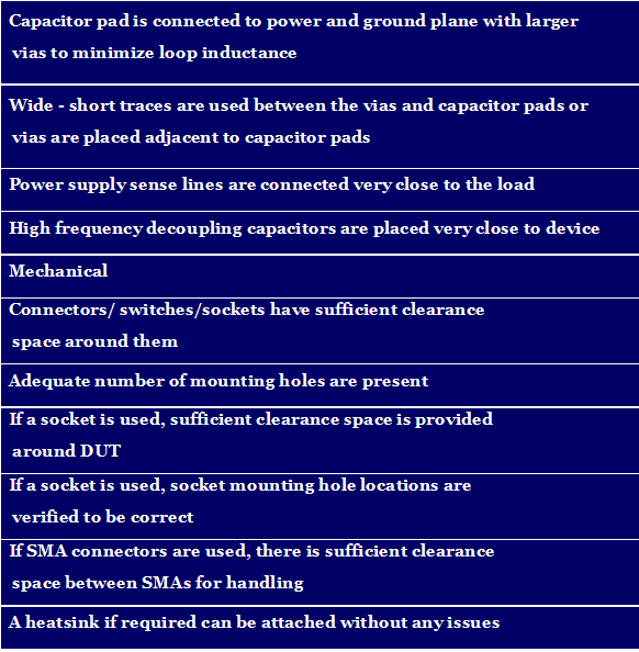
And finally, reference the sample checklists for PCB layout below:
Additional Resources:
If you are looking for more technical information or need to discuss your technical challenges with an expert, we are happy to help. Email us and we will arrange to have one of our technical specialists speak with you. You can also sign up for updates. Finally, please follow us on social media so we can keep in touch.