Technology 1T…Revolutionizing Memory Technology Again
Wednesday August 19, 2020By Mark Baumann
Director, Product Definition & Applications
MoSys, Inc.
As part of the design process for the MoSys Accelerator Engine Family of Blazar and Quazar products, a decision was needed as to what would be the best (in regard to size, speed and price) base (cell design) technology to utilize. The goal, as was stated in other blog and technology posts, was to build a product that had similar access parameters to that of QDR SRAM. At the same time be a cost-effective device that would provide 2x to 4x the density, of today’s QDR devices.
The initial choice was the settle on a memory cell design. The three options that were possible at the time were SRAM, DRAM and E-DRAM.
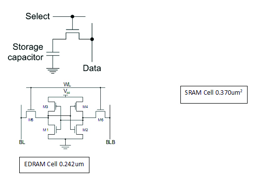
From a very high level the choice is SRAM at 6-transistors per cell, DRAM at 1 Transistor and a capacitor or E-DRAM which is a 1-Transistor and a capacitor cell but built using a Logic process. This decision has a direct impact on cell size and therefore the overall die size
Cell Design
The cell design that MoSys has chosen to use in the Blazar and Quazar product lines uses an embedded DRAM design. What MoSys feels is the benefits of this design vs either a straight DRAM or and SRAM cell is two-fold:
- By using an E-DRAM cell it is designed using a “logic” process at fabrication facilities like TSMC. By using a logic vs. a DRAM process the cell is slightly larger than a pure DRAM cell would be but the process, as it is named, also allows for integration of large amounts of Logic to surround the memory array, in the case where additional embedded functionality is desired.
- By using this version of the process, it is also possible to design the array with the desired characteristics to enable very fast access.
To achieve the desired speed (which in our case is close to SRAM speed) it is necessary to keep bit lines and word lines at a minimal length. This results in the capacitance of these metal lines used to run the word and bit lines of the array to be kept to a minimum, which in turn, defines the size of the line drivers and sense amps that will be needed to drive these lines. With respect to the MoSys devices, the array was designed with lines that had only 144 bits per line vs. the approximately 2000 bits per line that is standard in normal DRAM devices. This has the impact of reducing the load that both needs to be driven by line drivers and by the cells themselves when they are activated.
Reduced driver size. When the line drivers do not have to drive a large capacitive load the sizing of the drivers can be reduced. This has a positive effect in that the drivers can be smaller, but it has a slightly negative effect in that you need more of them to because they are driving smaller portions of the array.
Power is also impacted. When reviewing the power impact of utilizing E-DRAM, any one access will require less power than an access of a larger number of bits. The equation of P=CV2F is directly applicable. Since the C factor (capacitance) is reduced on any one access, by the need to drive shorter bit and word lines, the resultant power dissipation is reduced.
Power vs speed. As mentioned in the previous paragraph, the individual power of a single access is reduced, by reduction of the capacitive loads that need to be driven. By reducing the capacitance, the resulting speed is increased by being able to drive and recover the lines faster. This allows the array to run faster, which results in a higher bandwidth device. The impact of this is a slightly higher power dissipation in that the same P=CV2F equation now increases because the F (frequency) factor is increased. The result is still a reduction in power over an equivalent density of QDR devices.
Cell Size. An E-DRAM cell in 40nm TSMC process each takes approx. 0.242um2. Whereas a single SRAM cell in a comparable technology takes approximately 0.370um2, which is approximately 53% larger than the E-DRAM cell. When one places 576 M of these cells on a die it has a very large impact on overall die size. The E-Dram cell results in a die that is approx. half the size if the same density array in SRAM. (This is the major reason why even with newer technologies, the size of an SRAM cell will be the limiting factor in the density of the available arrays. The densest SRAM is 288Mb and DRAM are in the Gb and higher density).

The result of using this cell structure to be the basis of the MoSys Quazar MSQ220 (0.5Gb) and MSQ230 (1.1Gb) devices, is that one can achieve the density of 2X to 8X that of available SRAM devices at a comparable technology node. The device can run at comparable system speeds and achieve a lower power consumption than an equivalent SRAM and still be competitively priced.
Additional Resources
If you are looking for more technical information or need to discuss your technical challenges with an expert, we are happy to help. Email us and we will arrange to have one of our technical specialists speak with you. You can also sign up for updates. Finally, please follow us on social media so we can keep in touch.


