How Board Design Can Expedite Your Next Design Project
Friday May 14, 2021Part 1 of 2
By Mark Baumann
Director, Product Definition & Applications
MoSys, Inc.
MoSys recently hosted a webinar with our distribution partner Arrow. The focus was board design guidelines which, on the surface, appears to be a rather mundane topic. The reality is, however, that designing a board properly can save you time and money while accelerating time to market.
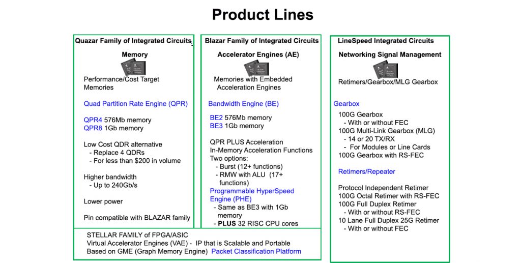
MoSys has developed a heightened interest in PCB design, based on the product offerings that have a strong dependency on the use of High-Speed SerDes, as seen in the following product offerings:
In our webinar, which can be viewed on the Arrow.com website, topics such as terminology commonly used in PCB designs that use SerDes, were discussed such as:
Insertion Loss which represents the loss of signal power resulting from the insertion of a device in a transmission line. Insertion loss is the ratio of the output signal to the input signal, and it is measured in decibels (dB).
Return Loss which is a measure in relative terms of the power of the signal reflected by a discontinuity in a transmission line. Along with the cause of this discontinuity such as any mismatch between the load connected to the line and the characteristic impedance of the line.
S-Parameters, or S (scattering) parameters can be used to characterize electrical networks In this case, scattering refers to the way traveling currents or voltages are affected when they meet a discontinuity in a transmission line.
Crosstalk which refers to the unwanted transfer of signals between communication channels.
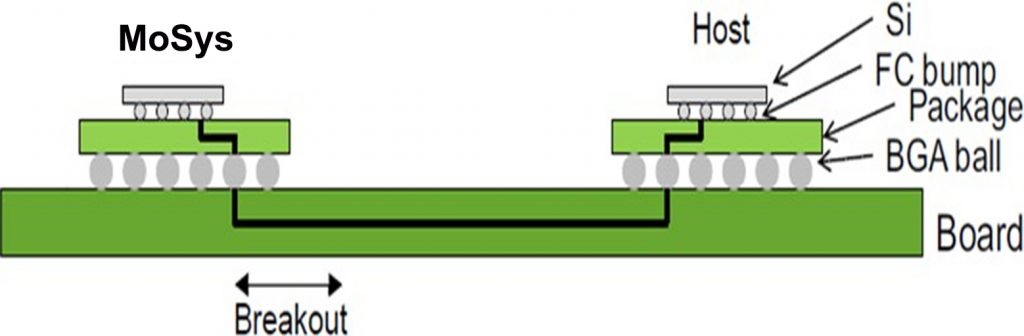
Channel Depiction:
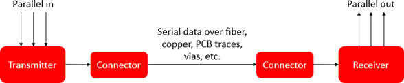
The definition of a Channel will include from the transmitting device die to the receiving device die. All devices including package, PCB material, etch, connectors, AC Caps etc. will all be important considerations in the channel design.
The following material are many of the areas of consideration when designing a high-speed PCB channel. The first of which is
PCB Material:
When it comes to PCB materials the following guidelines are considered by MoSys:
- Select the material with the lower loss to reduce signal attenuation from dielectric losses.
- Always choose lower Ɛr (dielectric constant) with a flat frequency response to reduce signal dispersion.
- Always choose a more densely woven fiberglass core and prepreg material surrounding the high-speed signal layers to minimize impedance and signal transmission variations.
- It is acceptable to choose less dense fiberglass styles for power layers and slower signal layers to reduce PCB cost
- Use wider traces (6 mil) and choose rolled copper foils over traditional electrodeposited (ED) copper
Other design elements to consider:
- Using fine trace widths down to 4 mils wide can improve routability, but narrow trace geometries increases conductor loss.
- Larger signal attenuation occurs for signals at 4 mils vs. 5 to 6 mils.
- For example, for a 28-Gbps signal, the difference in attenuation at the Nyquist frequency (14 GHz) is approximately 3 dB for 4 mils versus 6 mils wide trace.
Routing Practice:
· It is safest to keep signal separation and pair ground shielding while keeping in mind that wider traces are easier to maintain desired impedance and make it easier to support smooth gradual turns.
Via Design:
· Vias are a common source of channel discontinuity and dispersion.
· It is common for the characteristic impedance of differential vias to be lower than desired 100 Ω differential.
· Variations in both Capacitance and Inductance are seen with Via Design
· Minimize Cvia using the following techniques:
- Reduce the via capture pad size.
- Eliminate all non-functional pads (NFP)
- Increase the via anti-pad size to 40 or 50 mils.
- Minimize Lvia using the following techniques:
- Eliminate and / or reduce via stubs.
- Minimize via barrel length by routing stripline traces near the top surface layer and applying techniques like back-drilling to any unnecessary excess via length
In Part 2 of this blog we will cover trace matching, reverse polarity, AC coupler capacity, power integrity, channel design and first order considerations.
Additional MoSys Resources:
If you are looking for more technical information or need to discuss your technical challenges with an expert, we are happy to help. Email us and we will arrange to have one of our technical specialists speak with you. You can also sign up for updates. Finally, please follow us on social media so we can keep in touch.