MoSys LineSpeed™ Flex PHY Solutions – Successful Design and Bring-Up of a Serial Link
Thursday March 5, 2020By Scott Irwin
Vice President, LineSpeed Products
MoSys, Inc.
Designing, implementing, and validating a new, high-speed, serial communication link can be challenging. But with a step-by-step approach and attention to good signal integrity practices, getting to a successful implementation on the first design pass and minimizing time-to-market can be accomplished.
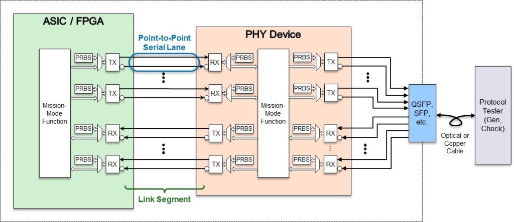
A typical serial link can be one device to another device, or it may traverse multiple devices that have been implemented in multiple technologies and may be supplied from multiple vendors. The serial connections between the devices include PCB, connector, and optical channel components. An example of such a link using multiple devices is illustrated in Figure 1, which includes an ASIC or FPGA component, a discrete PHY device, a pluggable connector (e.g. QSFP or SFP), and external equipment, such as a protocol tester.
A step-by-step approach to designing and validating such a link is the best strategy for a successful implementation. These steps can be summarized as follows:
- Schematic design review with PHY vendor(s) – Once the initial design is captured, the schematic should be reviewed for proper component connections. This includes reference clock selection and signaling type (e.g. LVDS, LV-PECL, etc.). The high-speed serial lane connections between each component should be checked, including voltage swing/DC compatibility, AC coupling (if needed), serial lane matching/swapping, or any polarity inversion within differential pairs. The power supply network should also be reviewed against supply voltage/ripple specifications.
- Layout review with PHY vendor(s) – Once the physical PCB layout is complete, it should be reviewed for proper signaling specs and best signal integrity practices. The layer stack should be checked that it meets target single-ended and differential impedance. The traces should have adequate shielding and GND planes/shields should have adequate connections (or “stitching”). Channel discontinuities should be minimized, including BGA package “escapes”, connector routing, or other elements in signaling path. MoSys provides layout guidelines for its high-speed serial products.
- Validate each serial link segment – Each independent serial lane and segment of the link should first be validated and tested for basic connectivity and signal integrity against the anticipated performance specification. This involves generating a PRBS pattern in each serial transmitter and checking it in each serial receiver. By doing so, the Bit Error Rate (BER) of each portion of the link can be validated on its own. The typical PRBS pattern used for networking is PRBS31. For NRZ links of 28Gb/s or below, error free operation should be expected for most IEEE or OIF industry standard chip-to-chip or chip-to-module connections. It is much easier to identify and debug potential issues such as differential polarity inversion, signal integrity problems, etc. by focusing on each segment/lane. Using loopback from one chip to another is also a common method but does not provide full visibility of the individual Tx/Rx connections.
- Validate complete serial link – Once each segment is validated to meet expected operating performance, then the “mission-mode” of the link can be established and validated. For example, this could involve enabling the higher layers of an Ethernet link and exchanging packets between network test equipment and the newly created design. If a segment-by-segment approach of confirming signal integrity as described in step 3 above was followed, the probability of success when turning on “mission mode” functions is much higher and can avoid wasting valuable time chasing after high-level issues only to find a single segment signal integrity or connectivity issue between devices.
With good signal integrity practices, design reviews, and a structured approach to bringing up and validating a high-speed serial communication link, the overall risk and time-to-market can be significantly reduced. At MoSys, we help our customers achieve first-pass success through our robust PHY products, design & layout guidelines, and direct application support throughout the path to production.
Additional Resources:
If you are looking for more technical information or need to discuss your technical challenges with an expert, we are happy to help. Email us and we will arrange to have one of our technical specialists speak with you. You can also sign up for updates. Finally, please follow us on social media so we can keep in touch.