Memory Controllers Part 2 of 2
Tuesday July 14, 2020By Michael Miller
Chief Technology Officer
MoSys, Inc.
Statistics (R-M-W)
In Part 1 of this blog, we discussed memory controllers in a broad context. Part 2 will delve into the micro architecture of MoSys memory controllers and statistics of R-M-W.
MoSys BE Statistic Controller
The BE interface performs the same bridge function between the application logic and the bandwidth engine device however it is designed to support R-M-W or read-modify-write operations in order to allow the application to issue ALU operations to perform functions such as maintaining statistics or metering. This design utilizes the large memories found in the BE2 or BE3 devices along with its embedded ALU and its RMW instructions in order to implement the counter or metering.
As an example, with the current BE2 memory size and 8 serial lanes running at 12.8 Gbps, this Statistic Controller has the following capabilities:
- Incrementing up to eight concurrent counters at the rate up to 160 Million counts per second which is higher than typical 100GE at 148.8 Mpps.
- The 576 Mb memory capacity on BE2 can support up to 8 x 256K counters.
- Interface to read the counters. This operation returns the counter content.
- These counters are lifetime counters (which means they are a full 64 bits wide).
- Counters are initialized by the controller after de-assertion of reset.
- Diagnostic interface to read and write BE2 memory for initial memory testing.
- Optional ECC Correction circuitry to correct one-bit error and detect two bits or more error on the counter read data.
Micro Architecture
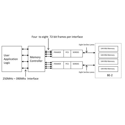
For a statistics and R-M-W operations, there are 8 counter interfaces in which four counters are mapped to lower part of the four partitions in BE memory and other four counters are mapped to upper part of the four partitions. The user specifies 18-bit counter index that is mapped to a location in partition. The figure 8 below illustrates the statistic controller interfaced with user at one end and GCI PCS/Framer at the other end.
The user requests are captured at the input of an Asynchronous FIFO at a clock frequency of the application logic. The R-M-W (or statistics) controller then pulls user requests out of this Asynchronous FIFO at its internal clock derived from SerDes clock. The statistic controller operates at this frequency to optimize the interface with GCI running at SerDes speed. The statistic controller creates RMW (Read-Modify-Write) commands from the user requests to implement counter operation using BE memory.
The statistic controller has following major blocks:
- Eight asynchronous FIFOs corresponding to 8 user increment requests.
- Eight asynchronous FIFOs corresponding to 8 users read count requests.
- One Asynchronous FIFO for memory Diagnostic interface user request.
- A scheduler block which performs RMW command formation and scheduling based on user request.
- A receive data block that receives the read data from the PCS/Framer block and send it to the user on its respective interface, this being the same interface that requested the action.
- A debug interface block that tests the BE memory.
On each wheel (or FPGA Cycle time), four counter operations are performed that is four R-M-W commands corresponding to counter increments, are scheduled. On one-wheel cycle, four counters located at lower part of four partitions in BE memory, are incremented. In next wheel cycle, another four counters located at upper part of four partitions, are incremented. Out of every 15 accesses of the BE memory, first 14 accesses are RMW commands corresponding to counter increments and 15th access is the memory read operation. The RMW and read command scheduling is shown in Figure 1 below.
Summary
MoSys memory controllers are designed to simplify the integration of the accelerator engines into a design. The controllers are built with all the high-speed SerDes control and implementation of the GCI protocol essentially “hidden away” from your design effort. MoSys controllers which have been deployed in the field since 2004 have been proven to be robust and reliable.
The interface which is presented to the user application interface is a straightforward Address, Data, Command bus structure, that is compatible with and easily adapted to an AXI interface. Multiple versions are available to support different access patterns and for different hosts (Xilinx, Intel, ASIC etc.)
This blog allows a user to realize that integration and implementation of the MoSys family of accelerator engines is not a long process and can be accelerated by utilization of the readily available MoSys IP.
Additional Resources:
If you are looking for more technical information or need to discuss your technical challenges with an expert, we are happy to help. Email us and we will arrange to have one of our technical specialists speak with you. You can also sign up for updates. Finally, please follow us on social media so we can keep in touch.