
Programmable HyperSpeed ICs
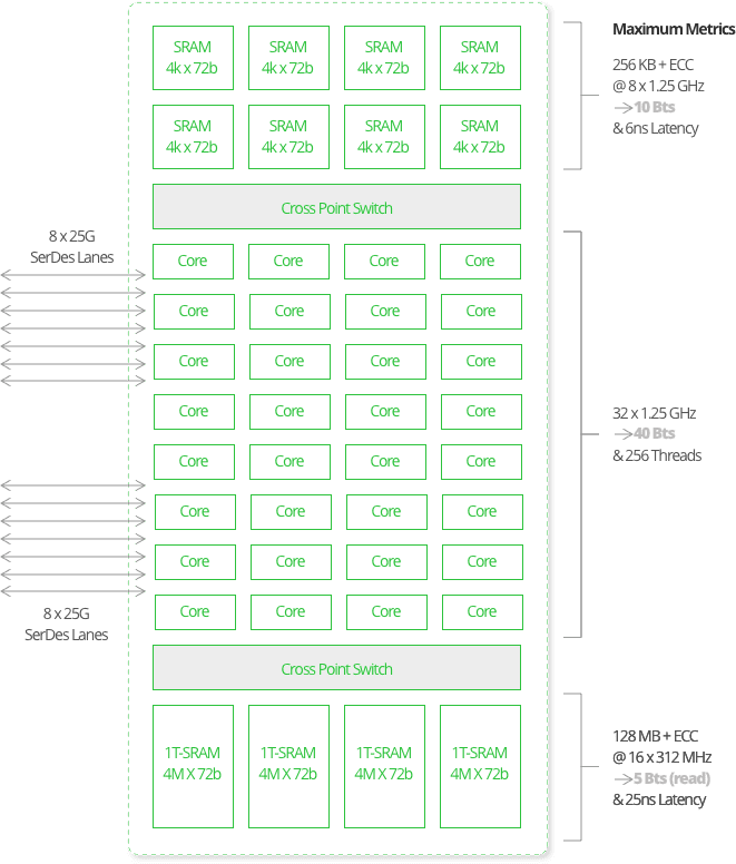
The PHE features four levels of memory, 32 Processor Engine (PE) that are Risc core processors with an Application Specific Instruction Set and a high speed serial I/O interface for low pins count/high signal integrity designs.

Programmable In-Memory RMW Functions
A huge leap in Application Acceleration is the ability to embed User Defined Functions. These can be specialized RMW functions such as sequential location counting, to full Algorithms for application such as sophisticated search, string pattern matching or data analysis.
Now you have the flexibility to program your application’s common and bandwidth-consuming functions to run in-memory. Using the power of the PE instruction set to create In Memory Functions, freeing up your system processor or FPGA to do other things and ensures your application achieves the maximum performance boost.
Or, just embed functions, as simple as a Read/Modify/Write, (where we insure that if the location being modified is trying to be Read, we hold off the Read until the Write is complete) to make the software architecture run smoother by not having to manage tasks that could better execute in the accelerator. Simplify your software!
What is embedded is up to the creativity of the Software Architect and how much you want to accelerate the application!
Processor Engines
Our Processor Engines (PEs) are risc based cores where we were able to customize an instruction set that is
- Application focused
- Would provide a high level of acceleration by executing In Memory
- Could simplify the overall software architecture by moving user defined functions (or algorithms) into the device
- Would allow optional multi-threaded functions
Multi-Level Memory Architecture and Density
Multi-level memory provides another level of speed customization. The HE has four levels that operate with the PE. Each level provides different speed options and data locations to best execute a function.
The heart of the memory IC is our advance, parallel array 1T-SRAM with a capacity of 1.152Gb of our patented 1T-SRAM.
- The memory is divided into 4 Partitions. Each partition has 128 banks allowing parallel (simultaneous) access.
- Since there are two independent I/O ports per device, several memory accesses as well as multiple functions can be executing at the same time.
- Can be used as a Dual-Port memory
- The tRC is 2.67 ns allowing up to 5 billion transactions per second.
There is additional block of memories that total 2.3Mb which have higher speed and even a third rank of faster register memories. Combined, it is possible to support a combined 24 Billion accesses.
This enables you to pick the speed path that best improves system performance!
Scheduler and Priority Domains
The Scheduler is important when you use the parallel execution capability. Scheduler manages simultaneous request execution to insure the outputs are in sync. The optional use of Domain Scheduling allows user to set function execution priority if that is important.
An additional feature of the PHE is DATA INTEGRITY OF A RMW function. When you are in the process of modifying a memory location with an RMW function, that there will be a request to read the location being modified. The Scheduler will pause the Read request UNTIL the RMW has been completed and the memory location has the most current, up to date value.
Easy to Design-In
- Fewer pins using serial I/O with the GigaChip Interface technology
- Clean and reliable signal integrity board layout
- Standard use as a QDR replacement
Simple to understand EIMF (Embedded In-Memory Functions) to accelerate performance
A lot of high speed random access memory, with easy to understand EIMFs, with so few signal pins.
Cannot get simpler than that!
High-Speed Serial Protocol I/O Interface
Our 16 SerDes lanes can transmit data up to 12.5Gbps, with an optional rate of 10Gbps. MoSys’ GigaChip Interface (GCI) delivers full duplex, CRC protected data throughput, enabling up to 10 Billion memory transaction per second on as few as 16 signals.
Traditional memory design requires a lot of interface pins (in some cases 1000’s of pins), making signal routing and integrity a design challenge.
Each Accelerator engine has 2 completely independent, 8 lane, I/O ports that allow simultaneous memory access operations.
Fixed In-Memory BURST Functions
The BURST Functions are focused on DATA MOVEMENT where they accelerate getting data in and out of the memory faster and more efficiently by reducing the number of commands.
The BURST Multi-Read/Multi-Write In-Memory Functions can combine up to 8 READS or 8 WRITES into a single BURST function. This reduces the number of memory accesses when moving data, nearly doubling the amount of data that can be moved with that same bandwidth.
And, the Accelerator Engine can do several BURST Functions simultaneously! Further increasing system performance.
Fixed In-Memory RMW Functions
The RMW Functions are focused on DATA COMPUTING where there is need for memory location modification involving RMW in applications such as counting, statistics, dual counter updates.
Normal memory location modification requires one command to READ a memory location, a second operation to MODIFY the value, and a third command to WRITE the new value back to the memory location.
The RMW Functions provide two levels of speed acceleration. First, the RMW functions can be executed with one command. Second, since the modification is executed within memory, there is no need to move the data out to be modified, and then back into memory to write. This removes all of the I/O latency.

1,152
Density (Mb)
2.67
tRC (ns)
BURST Embedded In-Memory Functions for superior bandwidth performance.
28
SerDes Rate (Gbps)
60
Latency (ns)
RMW Embedded In-Memory Functions for offloading common and repetitive functions to memory.
800
Buffer BW (Gbps)
20
Accesses (Bp/s)
Programmable Custom In-Memory Functions for enabling designers to fine tune memory specifically for their application.
Programmable HyperSpeed Engine Architecture
The PHE Has 4 Levels of Memory to Provide Maximum Acceleration

Cluster Architecture
The architecture of the PHE has the base structure of the BE3-RMW but allows Programmable Uwer Defined Functions by adding…
- User defined function controller
- The Cluster Array, made up of 32 Processor Engines
- A data path to move data into and out of the Cluster Array.
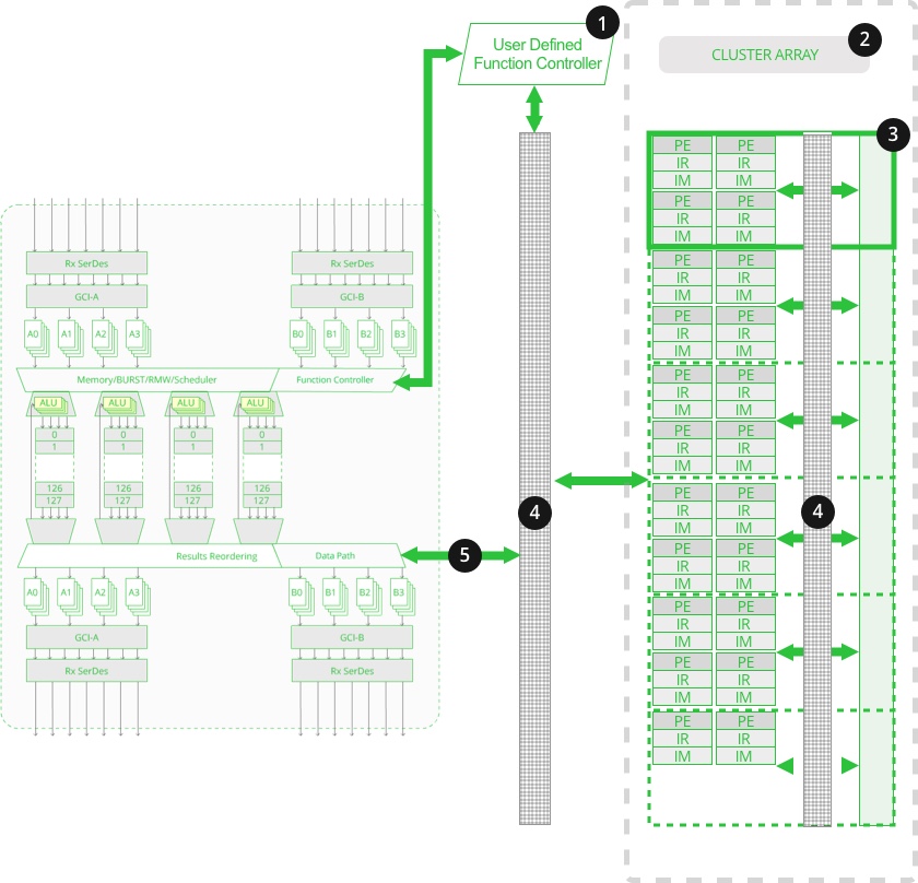
1. PE User Defined Function Controller
- Functions initiated from the I/O ports are directed to available threads on a PE in assigned pools for execution.
- Memory Access request from a PE to READ or WRITE to Main Memory.
2. Total Cluster Array
- 8 Clusters in the Cluster Array
- 32 PEs
- Combines all Local Cluster memories toa total of 32k x 72b Common Cluster memory accessible by all PEs
- 12 Billion memory transfers total
- 48 Billion instructions per second
3. A Cluster
- 4 PEs in each Cluster
- A PE has dedicated Instruction Memory and 128 x 72b General Purpose Registers
- 42x72b Local Cluster Memory
4. Cross Point Switches
- Tightly connects PEs to Main Memory and Cluster Memory
5. Data Path
- Added Data Path
Speed Path #2
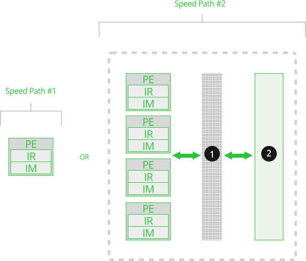
#2 The Cluster
- 4 PEs
- Cross Point Switch between PE and local Cluster Memory
- Local Cluster Memory
1. Cross Point Switch
- Tightly connects all 4 PEs with the Cluster Local Memory
2. Local Cluster Memory, Level 3
- 4k x 72b
- Latency 6ns
- tRC 0.677 ns
- 1.5 Billion transfers per second
Function Execution
Function Speed Path #2
- Function program is loaded into the PE’s IM
- Functions can execute with the Cluster’s Local Memory
Speed Path #3
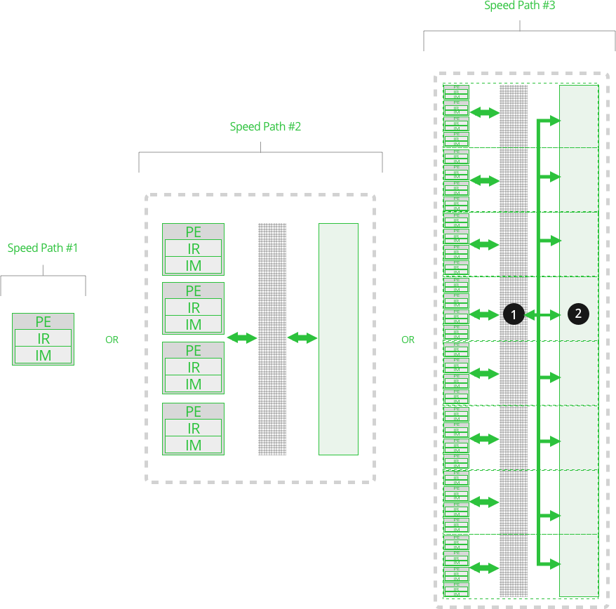
#3 The Cluster Array
- Combines 8 clusters together
- Total of 32 PEs
- Supports up to 256 threads
- Access to all device memories
- The Cross Point Switch is extended to all Local Cluster Memory which results in the total Cluster Memory becoming essentially one memory and accessible by all PEs
- 32k x 72b
- Any PE CAN access the Local Cluster Memory or any other Cluster
- 12 Billion access using all clusters
- Latency from 6ns to 12ns
- tRC 0.667ns
1. Cross Point Switch
- Extended Cross Point Switch connecting all Cluster local Cluster Memories
2. Total Cluster Memory, Level 2
- 32k x 72b
- All PEs have access to all of the Cluster Memories through the Cross Point Switch
Function Execution
Function Speed Path #3
- If a Function uses multiple PEs and data needs to be passed between Clusters, any PE can reach into the Local Cluster Memory of any other Cluster.
- 12 Billion maximum simultaneously transfer within the Cluster Array.
Speed Path #4
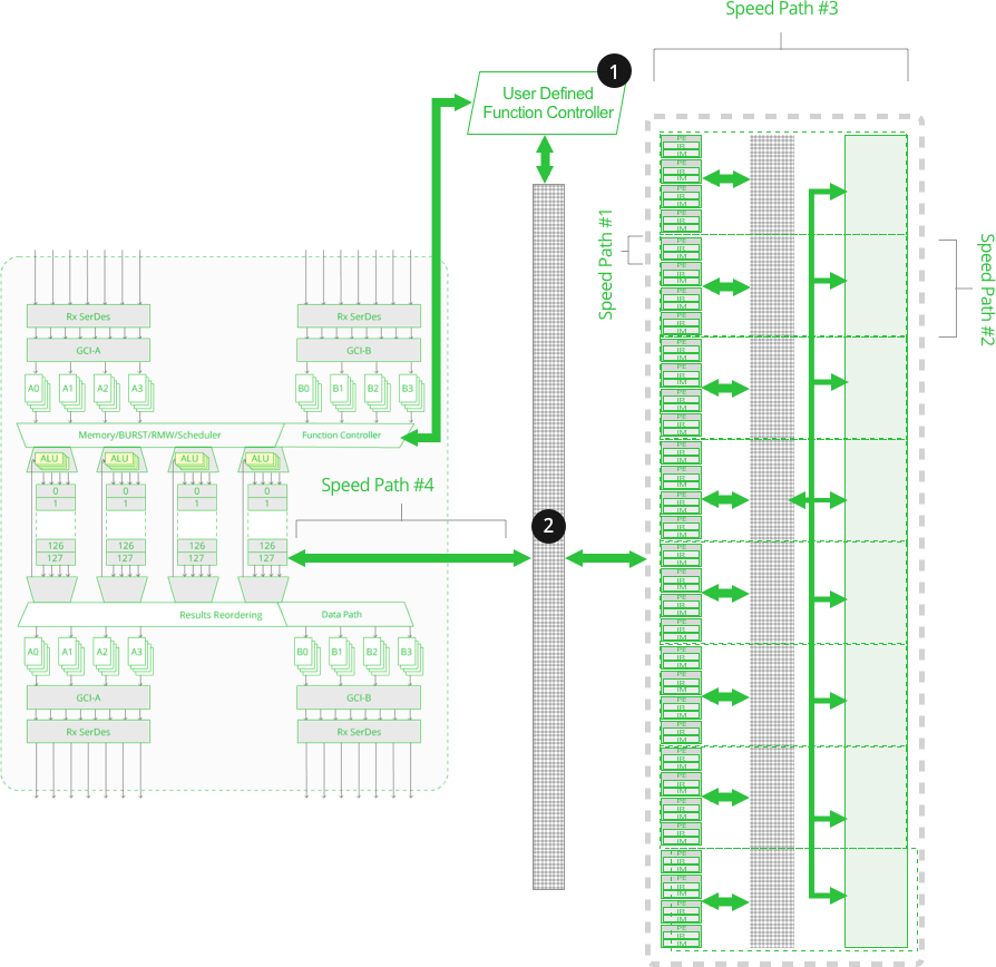
#4 The Main Memory, Level 1
- 1Gb of 1T-SRAM
- 4 Partitions of 128 Banks
- tRC 2.67n
1. User Defined Function Controller
- Functions initiated from the I/O ports are directed to the proper PE for execution.
2. Cross Point Switch
- Tightly connects the Cluster Array PEs to the Main Memory, Level 1 Memory
- Any PE can access any Main Memory location
- Latency as low as 25ns
- tRC 2.67ns
Function Execution
Function Speed Path #4
- Data to be operated on in a Cluster Function is written into a Main Memory location from an I/O transfer, where a PE can read it.
- Results from a Cluster Function is written into any main memory location allowing data to be externally read.
- 24 Billion maximum system simultaneous transfers (includes both transfer with the Cluster Array and between the Cluster and Main Memory.
The PHE’s Risc Cores Accelerate Your System’s Performance
32 Risc Cores
The HyperSpeed Engine allows a tremendous increase in application performance by the addition of 32 MPC (Multi-Threaded Processor Cores) Risc cores. The implementation of these cores improves your application’s performance by performing operations faster while reducing the demands on your FPGA or processor.
Accelerated Operation
The Risc cores are tightly coupled with a direct connection to the five levels of memory. Each level of memory has different speed performance specs, which means your can prioritize functions to the type of memory that better meets the need of your application.
Reducing Demands on Your FPGA
Every function you move into the HE, is one less function your FPGA or processor needs to perform. This means it can accelerate your system’s performance by prioritizing its resources on other functions. Your system can do more, do it faster, and get the job done using less power.
Customization
The ability to identify the time-consuming and repetitive functions that would benefit your applications performance, and then programming those to be performed within the HEP, means you can fine-tune the memory IC to meet the specific needs of your application.
Summary
Moving functions from the main application into the PHE delivers:
- Faster applicatioin execution
- Prioritized speed performance by allowing you to determine which level of memory is addressed
- Allows modification of data without having to transmit out-of and back into the Memory IC
- Frees up space and performance of an FPGA
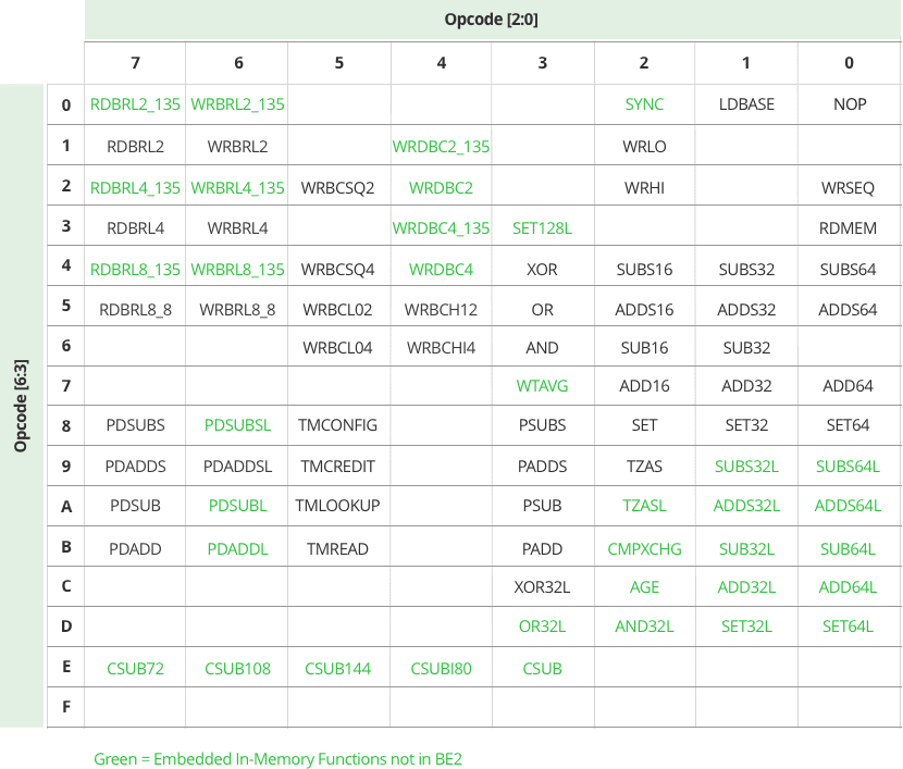
PHE Embedded in-Memory BURST and RMW Function Opcode Map
The PHE functions include all of the BE2 and BE3 BURST and RMW functions, as well as the CSUB functions.
PHE’s Risc Cores and Data Structures
Large Capacity Data Structure
- 128MB + ECC
- Parallel expansion
Tightly Coupled Cores and Memory
- Direct connect via cross point switch
- No cache –> no miss variability
Optimized Instruction Set
- Hash, Compressed Trie, etc.
- Packed bit fields
- 24 b x 24 b Multiplier
High Parallelism
- Up to 8-way thread cores
- 8-way threaded SRAM
- 16-way thread 1T-SRAM
Low Latency Memory Accesses
- 6 ns to 25 ns
- 4x faster than DRAM
- 2-level hierarchy possible